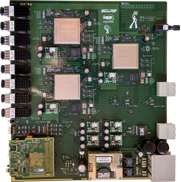
The electronics department has very pointed technical skills in various fields of analog and digital electronics. In this way, the laboratory deals with the full detector readout chain, from the low noise and consumption sensor readout, the signal sampling, the digital processing using fast programmable components, to the data distribution to the experiment acquisition system.
The electronics department developments can take place in harsh environments as in space or irradiated areas.
The department uses efficient tools and poeple’s expertise allow high technical projets. Thanks to high level courses, experts master simulation and CAD softwares.
The electronics department people is involved in international particule physics experiments.

Experts for physics experiments
The LAPP electronics department includes 11 research ingineers (ingénieurs de recherche), 3 study ingineers (ingénieurs d’étude) and 3 technicians (assistants ingénieurs). All work directly on experiment’s technical support. In the same time, 4 agents work a time fraction on general service functions: CAD, purchasing, devices and workshops.
The agents develop analog systems as low noise preamplification stages, shaping and filtering systems that allow the very high dynamics range detectors signals readout.
The makority of the agents develop acquisition systems. They design complex digital architectures that allow the sampling of the signals and their processing for the experiments: digital filtering, physical parameters calculation, triggers...
The department also includes micro-electronics experts. They contribute to analog and digital ASICs (Application Specific Integrated Circuit) developments for international projects.
Essential means for projects success
We use high-tech softwares, as the Cadence workflows.
![]() Integrated circuits design (schematics, routing, manufacturing files generation)
Integrated circuits design (schematics, routing, manufacturing files generation)
![]() Printed board design (schematics, routing, signal integrity checking...).
Printed board design (schematics, routing, signal integrity checking...).
![]() Design of complex architectures using programmables components as FPGA (simulation, VHDL&Verilog synthesis, placing&routing).
Design of complex architectures using programmables components as FPGA (simulation, VHDL&Verilog synthesis, placing&routing).
![]() Mixed signals designs simulation.
Mixed signals designs simulation.
In order to keep the best technical level and to master the new technics and skills, the department agents are involved in technological surveillance and follow courses (CNRS courses, IN2P3, Cadence...)
We have efficient devices that allow to test our developments: oscilloscopes, signal generators, network/spectrum analyzers... We master the test bench automation using Labview. We also have a milling machine dedicated to double sided printed boards prototypes and a workshop.
We teach in ingineer schools or IUT and in IN2P3 schools. Every year we welcome students from middle school to college. We regularly present our developments in collaboration meetings, international workshops or in papers.


